SWIR Cameras And Their Applications
SWIR videos
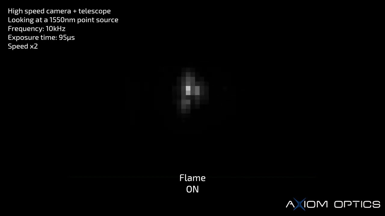
High-speed turbulence imaging of a point source at 1.5 µm using a high-speed SWIR camera and telescope. Acquisition made at 10 kHz with an exposure time of 85 µs and 14-bit pixel depth. In this example, the turbulence consists of induced scintillation with a heat source that changes the refraction index of air. Our high-speed SWIR InGaAs camera solutions are the ideal solution for use in fast adaptive optics and other setups used in FSO (Free-Space Optics) telecommunications.
Video made with: C-RED 3 High-Speed Uncooled InGaAs Camera
High-resolution imaging is now possible thanks to Sony’s IMX990 InGaAs chip with 1280 x 1024 px resolution and industry’ smallest pixel pitch of 5 µm. SWIR imaging allows high contrast imaging through atmospheric obscurants such as smog or fog.
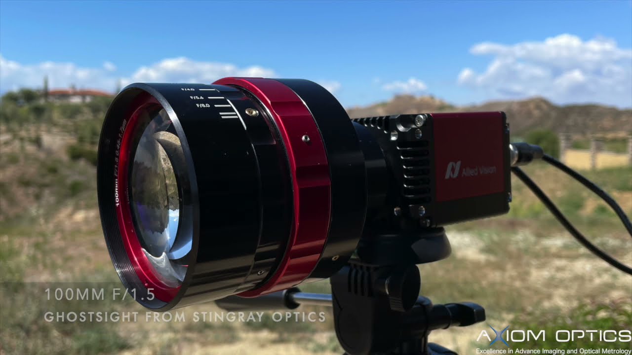
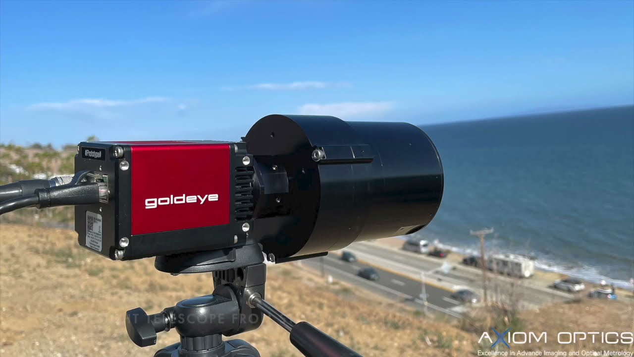
Video made with: Goldeye VSWIR G-130 TEC1 Camera
High-resolution imaging is now possible thanks to Sony’s IMX990 InGaAs chip with 1280 x 1024 px resolution and industry’ smallest pixel pitch of 5 µm. SWIR imaging allows high contrast imaging through atmospheric obscurants such as smog or fog.
Video made with: Goldeye VSWIR G-130 TEC1 Camera
High-speed imaging of water being poured in the short-wave infrared spectral range. 600 FPS achieved at VGA resolution and 14-bit pixel depth. Higher frame rates can be achieved by windowing down the sensor in both horizontal and vertical directions.
Video made with: C-RED 2 Cooled Scientific Camera
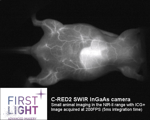
One of the biggest advantages of the SWIR range is that the auto fluorescence is negligible. This low level auto fluorescence increases the contrast and sensitivity compared to conventional imaging in NIR and visible ranges. Some of NIR fluorescence imaging contrast agents such as; ICG (indocyanine green), IRDye800CW and IR-12N3, has a non-negligible long tails passing 1500 nm region (NIR-II/SWIR) [1]. InGaAs (indium gallium arsenide) based SWIR cameras fill the gap for imaging in NIR-II/SWIR wavelength range (900-1700nm) where silicon detectors are no longer sensitive.
Video made with: C-RED2 Cooled InGaAs camera
- What is SWIR?
- SWIR vs eSWIR vs vSWIR
- Sensor Resolution and Pixel Pitch
- Laser Beam Profiling
- High-speed SWIR imaging
- FSO Telecommunications
- Small Animal Imaging
- Semiconductor Industry
- Recycling Industry
- Food Industry
- Metal & Glass Industry
- Agriculture
- Airborne Remote Sensing
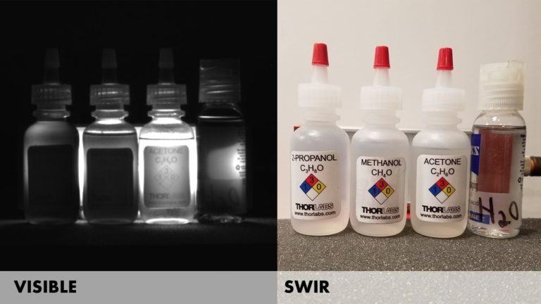
- Visible and SWIR Comparisons
What is SWIR or Shortwave Infrared?
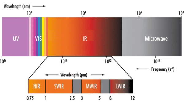
SWIR is the acronym for shortwave infrared and refers to non-visible light falling roughly between 1400 and 3000 nanometers (nm) in wavelength. The visible spectrum ranges from 400nm to 700nm, therefore SWIR light is invisible to the human eye. In order to detect SWIR wavelengths, we need dedicated sensors made of In GaAs (Indium Gallium Arsenide) or MCT (mercury cadmium Telluride) as silicon detectors are no longer sensitive to wavelengths larger than 1100 nm. In GaAs sensors are the primary sensors used in typical SWIR range. MCT is also an option and can extend the SWIR range, but these sensors are usually more costly and application dependent.
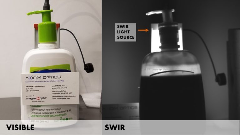
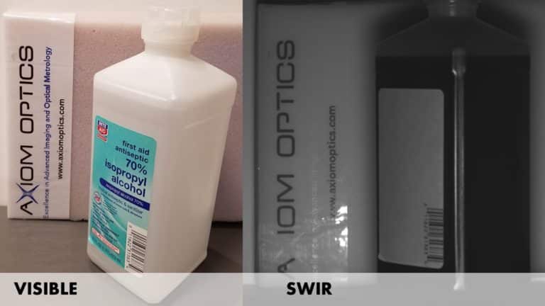
SWIR light interacts with objects similarly to visible light as it is reflective, consequently it exhibits shadows and contrasts in its imagery. Images from a SWIR camera are comparable to visible images in terms of resolution and detail.
Objects that are almost the same color while imaging in visible region can be easily differentiated using SWIR light, making objects easily recognizable. This is one tactical advantage of imaging in SWIR compared to visible region. Some of the natural emitters of SWIR are ambient star light and background radiance, therefore SWIR is an excellent application for outdoor imaging. Conventional quartz/halogen bulbs also act as a SWIR light source. Depending on the application, some sensors in SWIR cameras can be adjusted to have linear or logarithmic response to avoid saturation.
There are many advantages of using SWIR over a conventional visible sensor. Some applications that are not possible to image in visible range can be imaged using SWIR range. One example, is silicon wafer inspection, which is only possible due to silicon being transparent in the SWIR range. Other examples of materials that are transparent in SWIR region are; Sodium Chloride (NaCl) and Quartz (SiO2). Water vapor is also transparent in SWIR, making SWIR cameras more desirable when imaging through haze or fog. Applications where using SWIR is crucial are detailed in the following section.
SWIR vs eSWIR vs vSWIR
Because standard silicon-based sensors are typically sensitive up to 1000 nm only, SWIR cameras require sensors capable of imaging beyond the upper limit of silicon. InGaAs (indium gallium arsenide) sensors are conventionally used for SWIR imaging and cover the 900 nm to 1700 nm spectral range with high quantum efficiency (typically > 70%). Recent improvements to InGaAs sensors enable imaging both visible and SWIR (400 nm to 1700 nm using SenSWIR™ technology from Sony©, for example) or beyond the standard 1.7 µm cut-off with extended range solutions up to 2.2 µm.
To summarize, when it comes to short-wave infrared cameras:
– SWIR typically corresponds to the 900 – 1700 nm spectral range
-vSWIR or VIS-SWIR refers to the 400 – 1700 nm spectral range
– eSWIR or XSWIR or extended range InGaAs refers to cameras with a cut-off beyond 1.7µm; typically 1.9 or 2.2 µm.
Resolution and pixel pitch
InGaAs cameras bridge the gap between NIR wavelengths in the 950-1700 nm range, where silicon detectors are no longer sensitive. There is a still a gap however in the resolution of InGaAs sensors compared to that of silicon detectors, which can nowadays reach tens of megapixels and sometimes over 100 megapixels.
There are currently 3 ‘standard’ resolutions for SWIR InGaAs sensors on the market, with price increasing as the resolution goes up. Sensor pixel pitch is often related to the resolution with higher resolution sensors tending to have smaller pixels.
QVGA sensors offer a resolution of 320 (H) by 256 (V) pixels with a pixel pitch typically ranging from 20µm to 30µm.
VGA sensors are today the most standard resolution for InGaAs sensors with a resolution of 640(H) by 512 (V) pixels and a typical pixel pitch of 15µm.
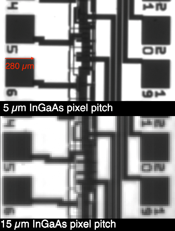
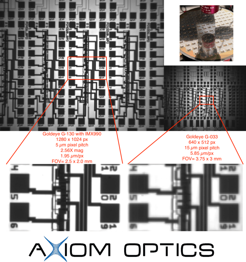
In 2021, Sony is releasing new sensors based on the SenSWIR technology with a pixel pitch of 5µm, making them the smallest pixel pitch on the market for InGaAs-based sensors. High resolution imaging is now possible with 1280 (H) x 1024 (V) or 640 (H) x 512 (V) resolution sensors with 5µm pixel pitch.
To find out more about our small pitch cameras, visit the products below.
Laser Beam Profiling
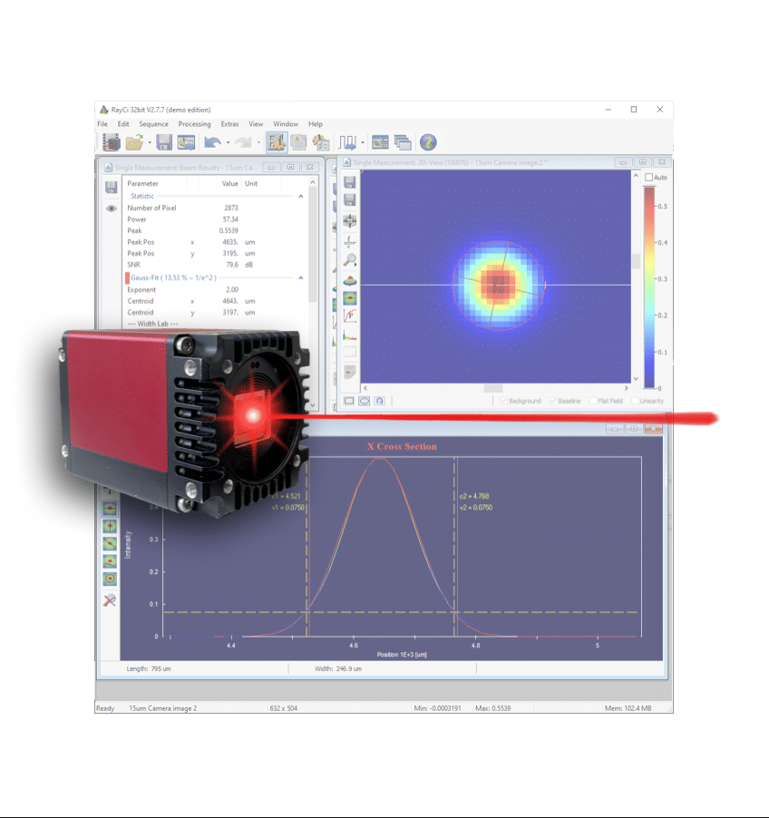
Measurement and analysis of laser-beam characteristics is essential for today’s laser-based applications. In general, beam characterization involves measurement of the beam spatial-energy density distribution, commonly known as the beam profile. Beam-profile analysis provides an understanding of the beam spatial characteristics such as size, shape, position, propagation, and mode structure properties. These measurements enable the required process-specific beam parameters, such as alignment, focus spot size, or beam uniformity (to name a few), to be achieved and maintained for optimum laser system performance.
For lasers with beams that are nearly collimated (paraxial), measurement of the beam-profile characteristics involves sampling the spatial distribution of the beam energy (or power) density in a plane (x and y-axis) perpendicular to the beam propagation path.
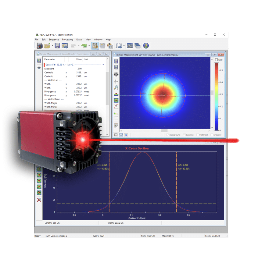
The advent of two-dimensional InGaAs detector arrays offers a viable approach for measurement of short-term beam-profile variations as opposed to scanning slit based systems. The individual sensors (pixels) in the detector arrays provide measurement of the energy density at discrete locations across the entire beam measurement plane while the entire array samples the beam simultaneously, thus providing a virtually instantaneous two-dimensional beam-profile data set (or beam image).
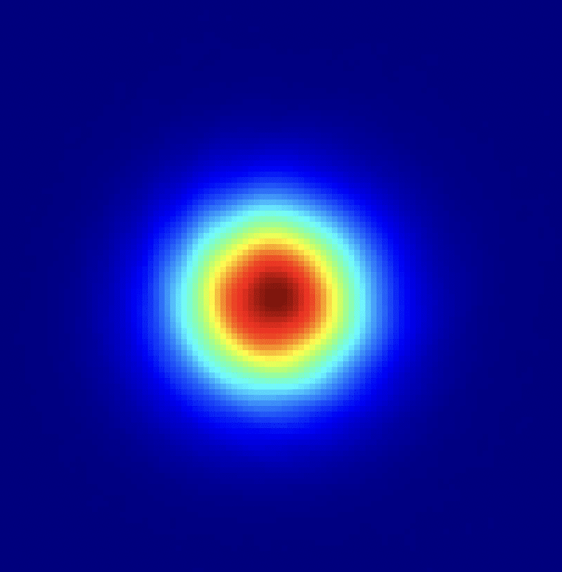
This approach can therefore capture the beam characteristics of a single laser pulse. When coupled to a computer, the detector-array data can be digitized and graphically displayed for qualitative visual inspection of the beam mode profile structure using a variety of beam profile plots. Numerical analysis of the profile data provides information such as:
- Position: peak position, centroid position;
- Relative total energy or power;
- Peak power or energy density;
- Width and diameter: knife-edge, slit, D86, second moment (D4σ), cross-section widths, fitted widths and more;
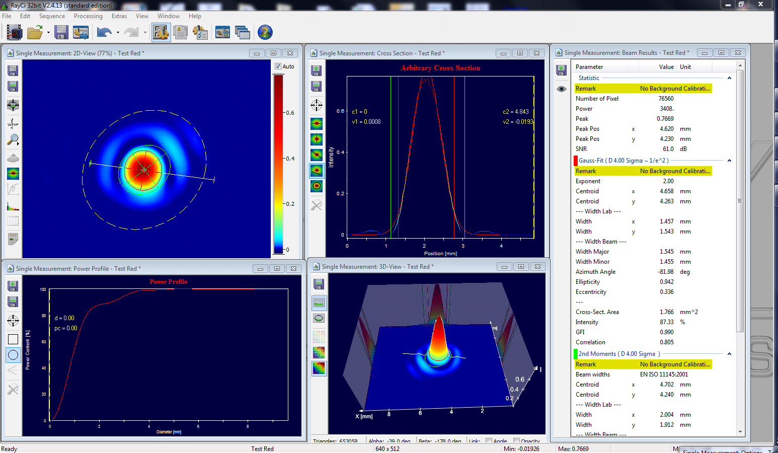
- Circularity/ellipticity, aspect ratio, beam orientation;
- Divergence (requires far-field optical set-up or a focusing lens)
- Propagation M2, beam parameter product (requires multiple profile measurements through beam waist).
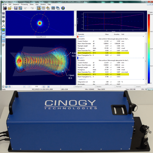
- Mode structure analysis: Gaussian fits, top-hat fits, uniformity, satellite or stray beams and more.
High-speed SWIR imaging
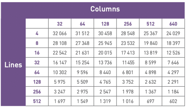
It is important to note that most manufacturers will display frame rate specifications corresponding to the best scenario, which in most case involves 8-bit data (Mono8 format). Because most SWIR InGaAs cameras have a native 14-bit ADC, not using the full pixel depth means compromising the data.
We offer the C-RED SWIR camera family with global shutter and high frame rate while always outputting data in 14-bit. No need to compromise on the pixel depth to go faster.
The table below shows the achievable frame rate as a function of image size with 602 Hz being the max frame rate at full resolution of 640 x 512 pixels.
Free Space Optical Telecommunications (FSO)
An FSO system in its simplest form is illustrated below. The data to be transmitted is converted to a binary format (1 and 0), then into light pulses (ON/OFF). A transmitter (laser source and focusing lens) sends the light pulses, aiming the direction of a receiver. The receiver collects the light pulses, which are then processed and converted. Note that the system can be used in the reverse direction. The system is interfaced at both ends with a physical network (cable, fiber). In more complex implementations, the laser beam can be modulated.
FSO can be used for ground to ground communication: outdoor wireless 2G/3G and 4G networks, to cover the edge of physical networks (“the last mile access”), CCTV surveillance networks, etc. More importantly, it can be used for ground to space (satellite) communications. FSO enables simultaneously establishing a large number of independent links with high throughput; two major advantages compared to the radio bandwidth which is limited by its low directionality and radio frequency throughput (< 40 GHz). For example, Earth-observation satellites only overpass ground stations for a couple of minutes per day, it is critical that the large amount of data they collected can be transmitted in a short amount of time. Even more so for military satellites which very often may only communicate with ground stations within a limited geographical zone. Finally, FSO is the best option for extra-terrestrial communication which may come in use in the next decades… In short, FSO is a fast-growing segment for telecommunications, both in civil and military fields.
FSO communications are limited by a series of factors. Fortunately, some can be overcome by using Short Wave InfraRed (SWIR) (900 – 1700 nm) rather than visible (400 – 700 nm) or Near InfraRed (700 – 900 nm) wavelengths. Optimized transmission Disturbances inherent to air/free space may influence the optical transmission:
- weather conditions such as fog, rain, snow…
- various other effects like water/dust absorption, scintillation, scattering
- physical obstruction: trees, birds or buildings.
These factors attenuate the transmitted signal, leading to a higher number of errors when detecting the signal. Laser power increase is not the solution as the laser power density is limited to class 1M in order to keep an eye-safe environment.
The use of SWIR band lasers is extremely pertinent because of their ability to go through obstacles such as fog or some types of plastics. The recent rise of eye-safe lasers in the SWIR band has allowed a major improvement. A camera based on an InGaAs detector array must be used at the receiver end, as visible cameras are not sensitive to SWIR wavelengths.
The following figures illustrate the advantage of using SWIR cameras in earth-to-earth and earth-to-space configurations. Visibility is increased compared to visible range imaging, demonstrating how SWIR signal propagates efficiently.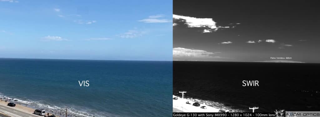
Small Animal Imaging in the NIR-II & SWIR
Small animal imaging is one of the main research areas for preclinical studies, including but not limited to; drug discovery, drug effectiveness, and early detection of cancer. Over time, imaging in the SWIR range became more profitable for scientists studying small animals. The short wave infrared (SWIR) range has several advantages compared to visible and infrared wavelengths in the domain of in vivo imaging. SWIR light provides higher depth of penetration while maintaining high resolution, low light absorption and reduced scattering within the tissue which makes it desirable to study living organisms. One of the biggest advantages of the SWIR range is that the auto fluorescence is negligible. This low level auto fluorescence increases the contrast and sensitivity compared to conventional imaging in NIR and visible ranges. Some of NIR fluorescence imaging contrast agents such as; ICG (indocyanine green), IRDye800CW and IR-12N3, has a non-negligible long tails passing 1500 nm region (NIR-II/SWIR) [1]. InGaAs (indium gallium arsenide) based SWIR cameras fill the gap for imaging in NIR-II/SWIR wavelength range (900-1700nm) where silicon detectors are no longer sensitive.
We recommend the following products for this application: C-RED2 Cooled InGaAs camera thanks to its low dark current and low readout noise.
Learn more by reading this application note.
Semiconductor Industry
The semiconductor industry has become one of the largest industries in the world and continues to expand. Manufacturing integrated circuits (ICs or chips) on thin silicon discs (wafers) is at the heart of this industry. Cameras with InGaAs sensors typically operate in the SWIR spectral range between 900 nm and 1,700 nm and can image through semiconductor materials such as silicon (Si) at wavelengths around 1,150 nm. Thus, they are an essential part of the inspection process. The ability to image through Si provides a non-destructive inspection method with great benefits for the production process. Today, the semi conductor industry integrates InGaAs cameras into testing, inspection, and quality control systems.
Silicon crystal and ingot brick inspection
Inspecting silicon crystals and ingots (also called bricks) is one of the classic applications for InGaAs cameras in the semiconductor industry. The ability to see through silicon at a wavelength range above 1,150 nm makes InGaAs cameras a well-suited solution for detecting inclusions such as impurities within a crystal or ingot, which can accumulate during the production process. The impurities are critical when sawing the ingots into thin wafers with a special diamond chain. If the chain strikes an inclusion such as a small piece of metal, the extremely expensive chain can break. Not only does replacing a chain carry a cost, but also leads to a lower productivity and a reduced profit. A SWIR camera can prevent this situation and thus ensure a smooth production process.
Wafer inspection or packaging
Another important application for SWIR cameras is the wafer inspection. During the manufacturing process of wafers, particles may occur on the top, at the bottom, and even inside or between the wafers. Whereas CCD or CMOS cameras detect particles on the top and at the bottom, InGaAs cameras see through the silicon and therefore detect particles between two bonded wafers. InGaAs cameras are also used for wafer packaging, where the alignment of the backside pattern to the front side of the wafer is conducted. The SWIR technology helps align layers of wafers as well as aligning other sub products such as ICs, memory cells, or transistors along the entire supply chain.
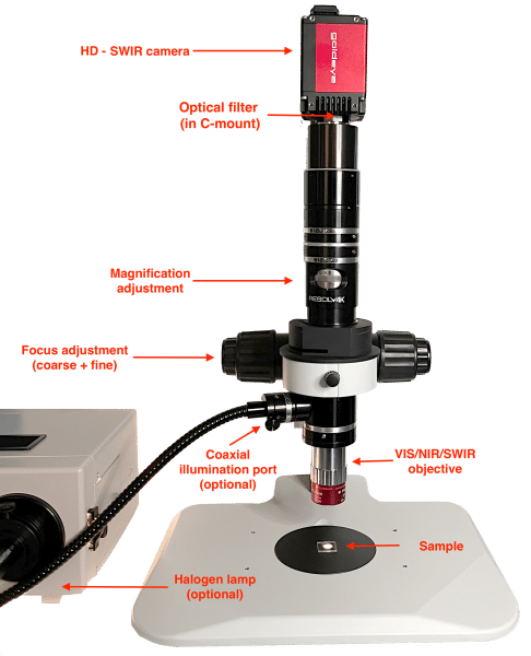
Example of Si wafer inspection using the HD-SWIR Digital Microscope. Images from Goldeye G-130 (IMX990 SenSWIR) and G-033 cameras.
Photovoltaics
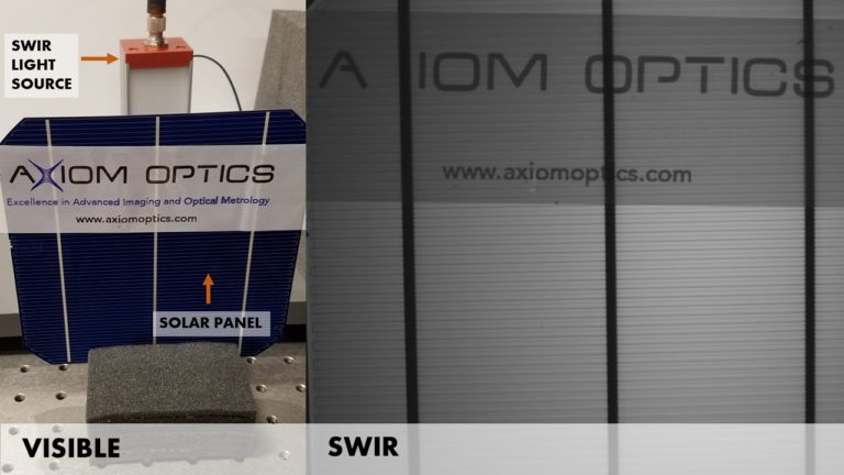
SWIR cameras can cover the inspection process of the whole supply chain from the silicon crystal to the ingots/bricks, wafers, solar cells, and finally the solar modules. Since InGaAs cameras image through silicon, they are the most effective solution to detect physical defects within the silicon. Besides SWIR imaging, which is a recent inspection technology, other important technologies and methods are common within the photovoltaics industry: Photoluminescence (PL) and electroluminescence (EL) are the usual methods for inspection purposes. PL imaging uses optical excitation (for example, laser illumination) to generate electron-hole pairs, which cause emissions by radiative recombination and thus can be detected by the camera. The band to-band emission around 1,150 nm provides information on defects and dislocation clusters inside the silicon. Moreover, mapping the defect-band luminescence at around 1,550 nm delivers results regarding the limit of the final cell efficiency. Therefore, the detection sensitivity of the InGaAs camera from 900 nm to 1,700 nm suits the application perfectly. In contrast, electroluminescence is the result of radiative recombination of electrons and holes in the silicon. Voltage is applied to the solar cell, which leads to a recombination with the available holes. The result is the emission of photons depending on the band-gap of the absorber material (silicon 1,150 nm). Besides crystalline silicon, other types of solar cells or module materials (also called thin film solar) can be inspected: Copper indium gallium diselenide (CIGS) is inspected at a wavelength of 700 nm to 1,330 nm (depending on the indium/gallium ratio) and copper indium diselenide (CIS) at a wavelength of 1,330 nm. The main advantage of SWIR over CCD and CMOS cameras is the shorter exposure time with an excellent quantum efficiency (QE) at the prime silicon emission wavelengths ensuring a quick characterization during the manufacturing process. CCD or CMOS cameras need longer exposure times with up to 30 seconds. Even NIR enhanced CCD sensors need exposure times of up to 3 seconds or more. In contrast, SWIR cameras need only a few milliseconds and thus significantly accelerate the production.
(Reference: Short-wave infrared (SWIR) cameras offer versatile application fields in machine vision)
Recycling Industry
The quantities of waste produced throughout the developed countries are growing continuously while the available resources are becoming scarce; hence, it is necessary to develop efficient methods to separate quality recyclable materials from collected waste.
Plastic sorting
Since all plastic waste looks alike in the visible spectrum, it is impossible to separate the recyclable material with conventional methods. In the short-wave infrared range, however, the absorption spectrum of different plastic materials shows different characteristics. Thus, the SWIR camera technology allows implementing automated separation systems to segregate material of similar quality and properties for recycling. By using latest SWIR cameras with an extended spectral range up to 2.5µm even further material types can be distinguished. To efficiently realize an automated waste separation process, the material is shredded into small flakes of similar size. A conveyor belt transports the flakes to the inspection unit, which consists of an illumination system and an SWIR camera with an InGaAs sensor. Since each plastic material shows unique spectral characteristics within SWIR, the different materials can be distinguished from each other and the spectral characteristics can be assigned to the corresponding plastic type. The different plastic types are separated on the conveyor belt by an array of airjets. To reach a fine screening and thus a good recycling rate with a high-quality outcome, this step can be repeated several times.
(Reference: Short-wave infrared (SWIR) cameras offer versatile application fields in machine vision)
Food Industry
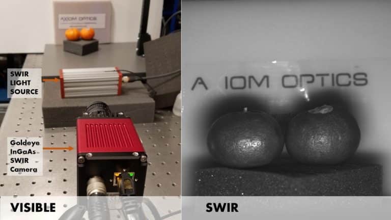
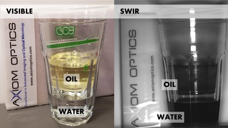
Fruits and vegetables contain between 80 % and 90 % water. Therefore, their spectral response is primarily characterized by the water absorption band, which has a peak at around 1,450 nm. Due to its stronger absorption, the water appears darker in the SWIR band.
Food analysis and sorting
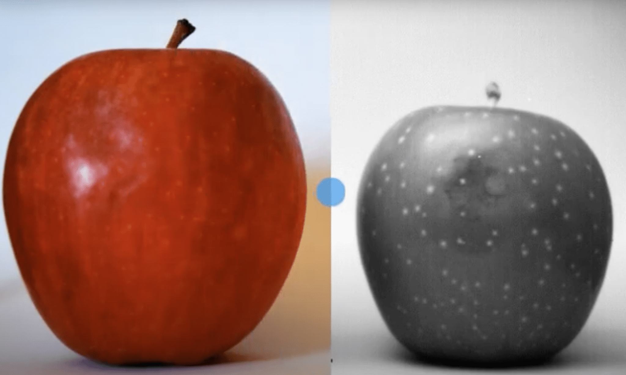
Each food product has a unique chemical composition and thus unique spectral characteristics in the visible as well as in the SWIR spectrum. SWIR cameras with InGaAs sensors are used for inline food inspection via conveyor belts. One of the most common approaches for analyzing food is spectroscopy. However, the latest development in the food industry shows the trend towards hyper and multi spectral imaging. This method combines digital imaging with spectroscopy to obtain detailed information across multiple ranges of the electromagnetic spectrum. The reflections and absorptions of certain wavelengths depend on the chemical composition and the molecular structure of the food. SWIR cameras are typically used in push broom imaging systems in combination with a spectrograph (hyperspectral imaging). If the number of bands to distinguish between certain materials is lower (<10) multi bandpass filters or dedicated illumination can be used (multi-spectral imaging). With their typical wavelength range from 900 nm to 1,700 nm, SWIR cameras can provide more spectral information than CCD or CMOS cameras. One example is the sorting of bruised apples. SWIR cameras can detect bruises, which are darker in the image because of their higher water content. This eases sorting them out for juicing and separating them from those with perfect characteristics to be sold to end customers.
(Reference: Short-wave infrared (SWIR) cameras offer versatile application fields in machine vision)
Metal & Glass Industry
SWIR cameras can be used for thermal imaging of hot objects between 250°C and 800°C. The metal and glass industry integrates SWIR cameras into process and quality control systems.
Molten metal process monitoring and inspection
In contrast to CCD and CMOS cameras, the spectral range of a typical InGaAs camera of 900 nm to 1,700 nm enables the inspection of emission differences between hot metal and slag. The information is used to detect differences in the slag within the manufacturing process. This ensures a maximized yield without any contaminated material.
Glass bottle monitoring and inspection
During the manufacturing process of bottles, InGaAs cameras enable an inside and outside inspection of the glass bottles. Because of their ability to perform thermal imaging of hot objects between 250°C and 800°C, SWIR cameras can monitor the temperature uniformity and the cooling rate of the glass. Thus, manufacturers can continuously observe the production to maximize the yield and the quality.
(Reference: Short-wave infrared (SWIR) cameras offer versatile application fields in machine vision)
Agriculture
Spectral imaging is also used for agricultural purposes, especially in combination with an unmanned aerial vehicle (UAV). Farmers can inspect plants from the air, for example, their strawberry fields: Looking at the SWIR image, the farmers can recognize plants or areas that lack water, have an ideal water content, or too much water. The more water is detected, the higher the absorption peak at a wavelength of 1,450 nm and the darker the area appears in the image. Therefore, for this type of application often a narrow 1450 nm bandpass filter is used to enhance this effect.
(Reference: Short-wave infrared (SWIR) cameras offer versatile application fields in machine vision)
Airborne Remote Sensing
UAVs are particularly popular in agriculture, but can also be used for many other purposes; numerous materials can be inspected from the air. Each inorganic material has a different chemical composition and crystalline structure resulting in a unique spectral response corresponding to its specific light absorption characteristics.
Geology and mineral inspection
The unique spectral response enables to perform a mineral mapping of every area in the world. Furthermore, forestry companies can map woodland from the air. Hyperspectral imaging contributes to geology and mineral inspection by methods similar to food analysis.
(Reference: Short-wave infrared (SWIR) cameras offer versatile application fields in machine vision)

