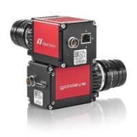
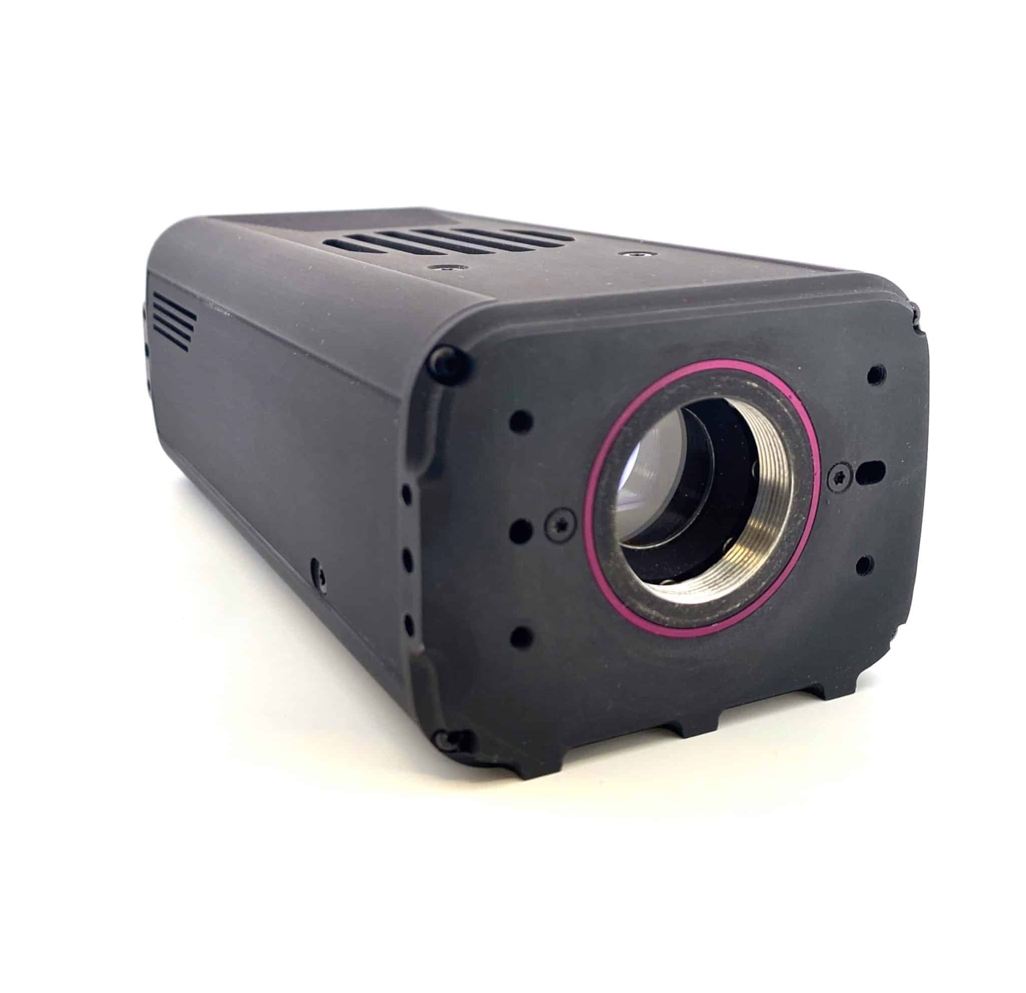
What is a Shortwave Infrared or SWIR Camera?
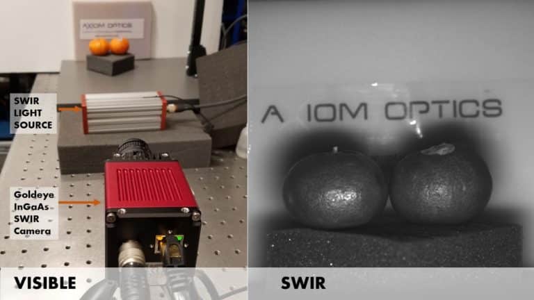
A SWIR (short for shortwave infrared) camera is a specialized imaging device that can detect non-visible light falling roughly between 1400 and 3000 nanometers (nm) in wavelength. Because the visible spectrum ranges from 400nm to 700nm, a SWIR camera can capture images that are invisible to the human eye. In order to detect SWIR wavelengths, SWIR cameras utilize dedicated sensors made of Indium Gallium Arsenide (InGaAs) or Mercury Cadmium Telluride (MCT), as silicon detectors are no longer sensitive to wavelengths beyond 1100 nm. InGaAs SWIR cameras are the primary tool used in typical SWIR range. MCT cameras can extend the SWIR range, but these sensors are usually more costly and application specific.
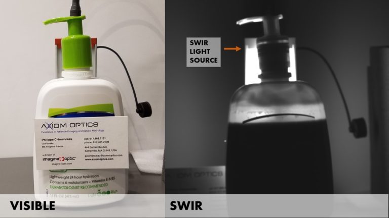
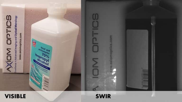
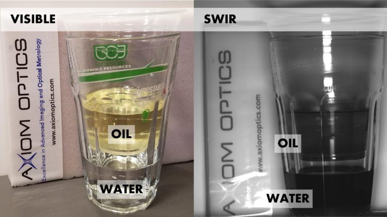
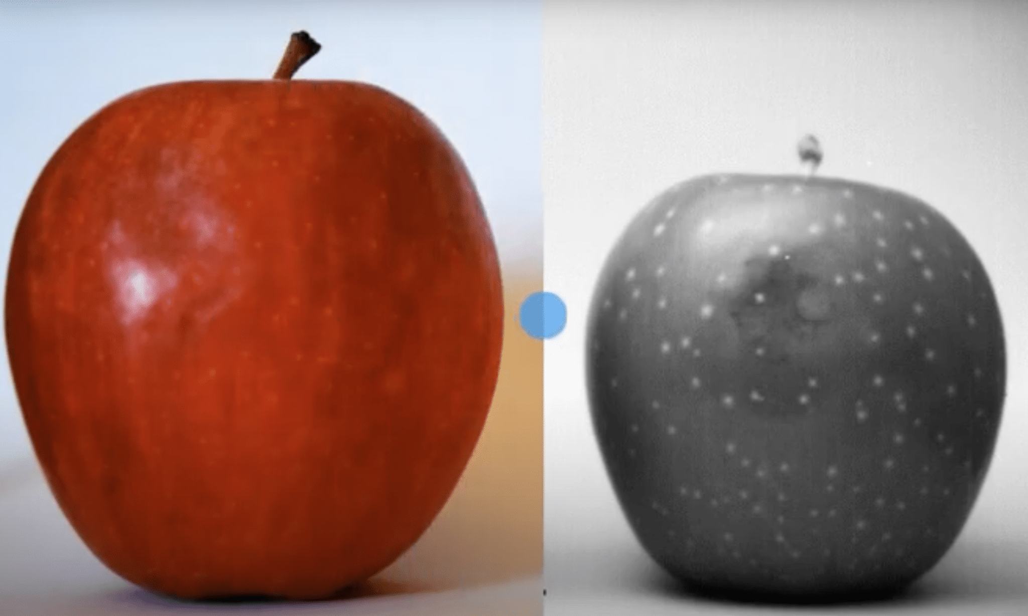
SWIR light interacts with objects similarly to visible light as it is reflective, consequently it exhibits shadows and contrasts in its imagery. Images from a SWIR camera are comparable to visible images in terms of resolution and detail.
Advantages of Using a SWIR Camera
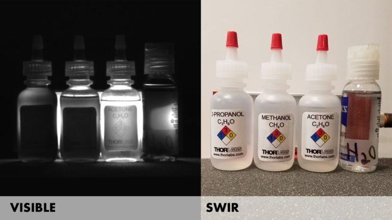
There are many advantages to choosing a SWIR camera over a conventional visible sensor. Objects that are almost the same color while imaging in the visible range can be easily differentiated using SWIR light, making objects easily recognizable. This is one tactical advantage of imaging in SWIR compared to the visible region. Because a SWIR camera can utilize natural emitters like ambient starlight and background radiance, it is an excellent tool for outdoor night imaging. Conventional quartz/halogen bulbs also act as a SWIR light source. Depending on the application, some sensors in SWIR cameras can be adjusted to have linear or logarithmic response to avoid image saturation.
There are some applications that are not possible to image in the visible range, therefore a SWIR camera must be used. One example is silicon wafer inspection, which is only possible because silicon is transparent in the SWIR range. Materials such as Sodium Chloride (NaCl) and Quartz (SiO2) are also transparent to a SWIR camera. Because water vapor is also transparent in this range, a SWIR camera is more desirable for imaging through heavy haze and fog.
Applications where using SWIR is crucial are detailed below.

SWIR vs MWIR and LWIR
The fundamental difference lies in whether the sensor detects reflected light or emitted heat. SWIR behaves most like visible light because it relies on photons bouncing off surfaces; this allows it to capture high-resolution details and “see” through atmospheric haze while still showing shadows and textures. In contrast, MWIR (Mid-Wave Infrared) and LWIR (Long-Wave Infrared) are thermal bands that detect the energy objects naturally radiate. While MWIR is prized for its high contrast and ability to track hot targets like engines over long distances, LWIR is the standard for “total darkness” thermal imaging, as it excels at mapping the ambient heat signatures of people and buildings without needing any external illumination. For more information, visit our blog post The Differences Between SWIR, MWIR, and LWIR Cameras.


High-speed imaging with a SWIR camera
Most standard SWIR cameras are restricted to frame rates between 100 and 200 Hz at full resolution. While users can “window” (select a Region of Interest) to increase speed, this often comes with technical caveats. For many sensors, only reducing the number of rows—not columns—actually improves the frame rate.
Furthermore, many manufacturers achieve their “top speeds” by dropping to 8-bit data (Mono8). Since most SWIR InGaAs cameras use a native 14-bit ADC, this high-speed mode forces you to sacrifice data precision for performance.
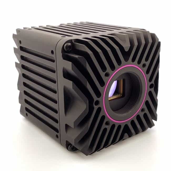
The Solution: C-RED Series
The C-RED SWIR camera family eliminates the need to choose between speed and depth. Featuring a global shutter, C-RED cameras maintain a native 14-bit output even at their highest speeds.
As shown in the table below, the C-RED series achieves a market-leading 602 Hz at full resolution (640 x 512), ensuring you never have to compromise your data to meet your timing requirements.

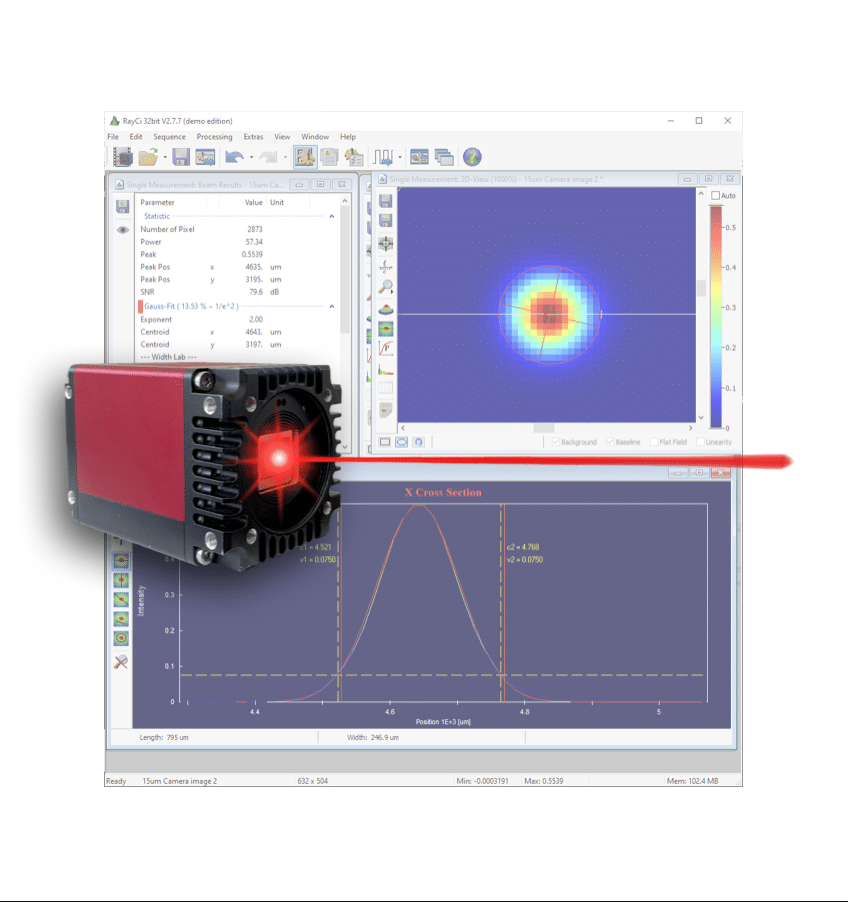
Laser Beam Profiling
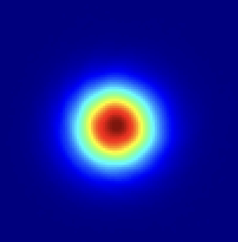
Precise measurement and analysis are the backbone of modern laser applications. By using a SWIR camera to capture the spatial-energy density distribution (the beam profile), you gain a comprehensive understanding of critical characteristics:
-
Spatial Properties: Size, shape, position, and mode structure.
-
System Performance: Real-time data on alignment, focal spot size, and beam uniformity.
Monitoring these parameters ensures your laser system operates at peak efficiency and maintains the specific beam quality required for your process.
Real-Time 2D Analysis
For nearly collimated (paraxial) lasers, a SWIR camera captures the energy density across the x and y axes, perpendicular to the beam’s path.
Compared to traditional scanning-slit systems, two-dimensional InGaAs detector arrays offer a superior approach:
-
Simultaneous Sampling: Every pixel in the array measures energy density at the same time.
-
Instantaneous Data: Unlike a moving slit, the array provides a complete 2D data set (beam image) virtually instantly.
-
Short-term Variation: This high-speed, simultaneous capture is essential for analyzing rapid fluctuations or “jitter” in the beam profile.
This approach can therefore capture the beam characteristics of a single laser pulse. When coupled to a computer, the SWIR camera data can be digitized and graphically displayed for qualitative visual inspection of the beam mode profile structure using a variety of beam profile plots. Numerical analysis of the profile data provides information such as:
- Position: peak position, centroid position
- Relative total energy or power
- Peak power or energy density
- Width and diameter: knife-edge, slit, D86, second moment (D4σ), cross-section widths, fitted widths and more…
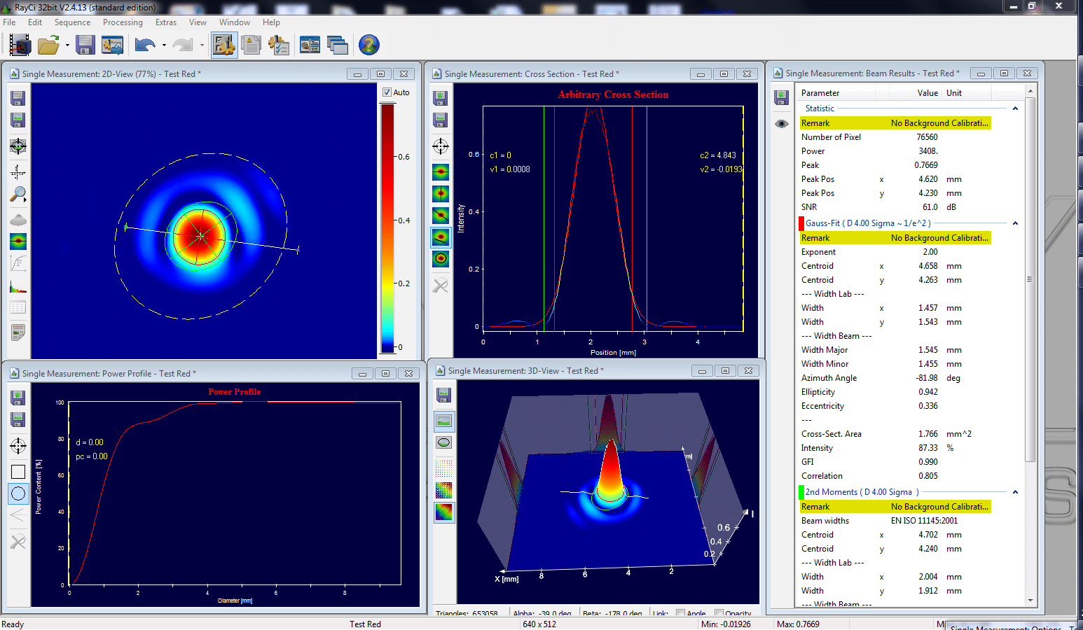
- Circularity/ellipticity, aspect ratio, beam orientation;
- Divergence (requires far-field optical set-up or a focusing lens)
- Propagation M2, beam parameter product (requires multiple profile measurements through beam waist).
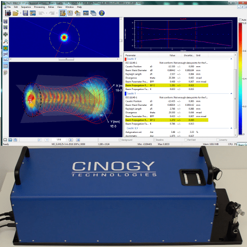
- Mode structure analysis: Gaussian fits, top-hat fits, uniformity, satellite or stray beams and more.
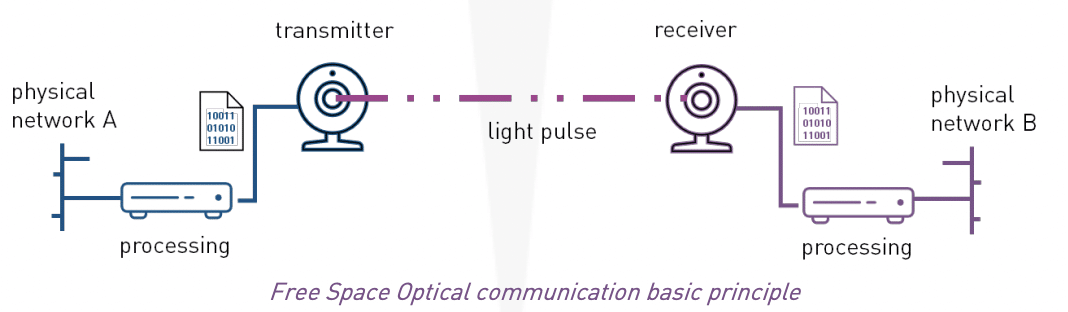
Free Space Optical Telecommunications (FSO)
An FSO system in its simplest form is illustrated below. The data to be transmitted is converted to a binary format (1 and 0), then into light pulses (ON/OFF). A transmitter (laser source and focusing lens) sends the light pulses, aiming the direction of a receiver. The receiver collects the light pulses, which are then processed and converted. Note that the system can be used in the reverse direction. The system is interfaced at both ends with a physical network (cable, fiber). In more complex implementations, the SWIR camera acts as the core of the receiver system, tracking and capturing the modulated laser beams across vast distances.
FSO is used for ground to ground communication, such as outdoor wireless 2G/3G and 4G networks, to cover the edge of physical networks (“the last mile access”), and CCTV surveillance networks, etc. More importantly, it can be used for ground to space (satellite) communications. FSO enables simultaneously establishing a large number of independent links with high throughput; two major advantages compared to the radio bandwidth which is limited by its low directionality and radio frequency throughput (< 40 GHz). For example, because Earth-observation satellites only overpass ground stations for a couple of minutes per day, it is critical that the large amount of data they collected can be transmitted in a short amount of time. Even more so for military satellites which very often may only communicate with ground stations within a limited geographical zone. Finally, FSO is the best option for extra-terrestrial communication which may come in use in the next decades… In short, FSO is a fast-growing segment for telecommunications, both in civil and military fields.
Overcoming Atmospheric Challenges with SWIR Cameras
FSO communications are often limited by atmospheric disturbances like fog, rain, snow, and scintillation (air turbulence). These factors attenuate signals, leading to data errors. Increasing laser power is not an option due to Class 1M eye-safety regulations.
The use of a SWIR camera is the definitive solution to these challenges. Because SWIR band lasers can penetrate fog, haze, and some plastics far more effectively than visible light, SWIR camera-based receivers ensure a stable connection where visible systems would fail.
Because standard visible cameras cannot detect these eye-safe wavelengths, a dedicated SWIR camera equipped with an InGaAs detector array must be used at the receiver end.
The following figures illustrate the advantage of using SWIR cameras in earth-to-earth and earth-to-space configurations. Visibility is increased compared to visible range imaging, demonstrating how SWIR signal propagates efficiently.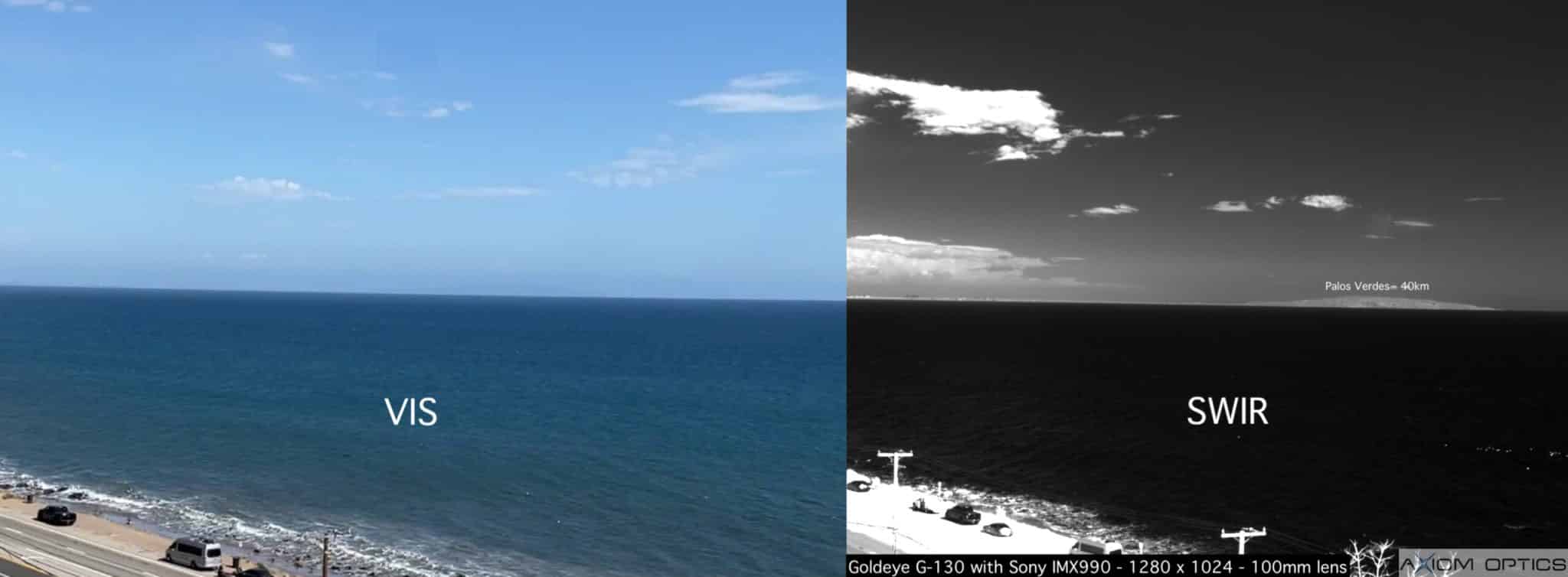
Semiconductor Industry
The semiconductor industry has become one of the largest industries in the world, centered on manufacturing integrated circuits (ICs or chips) on thin silicon discs (wafers). InGaAs SWIR cameras are essential tools in this field because they operate in the 900 nm to 1,700 nm range, where silicon (Si) becomes transparent (typically above 1,150 nm). By utilizing a SWIR camera, manufacturers can perform non-destructive internal inspections that are impossible with standard visible cameras. Today, the semi conductor industry integrates InGaAs cameras into testing, inspection, and quality control systems.
Silicon crystal and ingot brick inspection
Inspecting silicon crystals and ingots (also called bricks) is one of the classic applications for InGaAs cameras in the semiconductor industry. The ability to see through silicon at a wavelength range above 1,150 nm makes InGaAs SWIR cameras a well-suited solution for detecting inclusions such as impurities within a crystal or ingot, which can accumulate during the production process. The impurities are critical when sawing the ingots into thin wafers with a special diamond chain. If the chain strikes an inclusion such as a small piece of metal, the extremely expensive chain can break. Not only does replacing a chain carry a cost, but also leads to a lower productivity and a reduced profit. A SWIR camera can prevent this situation and thus ensure a smooth production process.
Wafer inspection or packaging
Another important application for SWIR cameras is the wafer inspection. During the manufacturing process of wafers, particles may occur on the top, at the bottom, and even inside or between the wafers. Whereas CCD or CMOS cameras detect particles on the top and at the bottom, InGaAs cameras see through the silicon and therefore detect particles between two bonded wafers. InGaAs cameras are also used for wafer packaging, where the alignment of the backside pattern to the front side of the wafer is conducted. The SWIR technology helps align layers of wafers as well as aligning other sub products such as ICs, memory cells, or transistors along the entire supply chain.
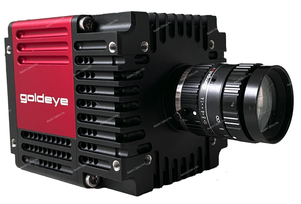
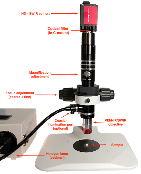
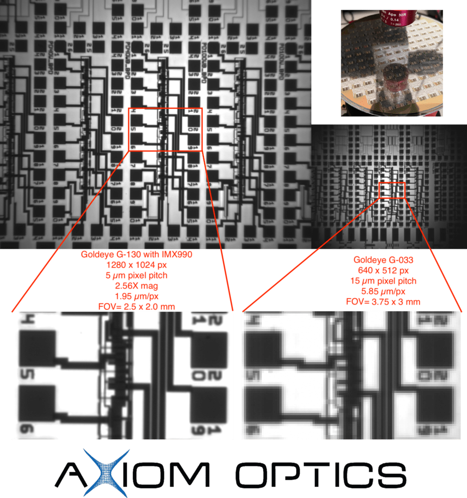
Below is an example of Si wafer inspection using the HD-SWIR Digital Microscope. Images from Goldeye G-130 (IMX990 SenSWIR) and G-033 cameras.
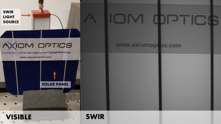
Photovoltaics
SWIR cameras can cover the inspection process of the whole supply chain from the silicon crystal to the ingots/bricks, wafers, solar cells, and finally the solar modules. Since InGaAs cameras image through silicon, they are the most effective solution to detect physical defects within the silicon. Besides SWIR imaging, which is a recent inspection technology, other important technologies and methods are common within the photovoltaics industry: Photoluminescence (PL) and electroluminescence (EL) are the usual methods for inspection purposes. PL imaging uses optical excitation (for example, laser illumination) to generate electron-hole pairs, which cause emissions by radiative recombination and thus can be detected by the camera. The band to-band emission around 1,150 nm provides information on defects and dislocation clusters inside the silicon. Moreover, mapping the defect-band luminescence at around 1,550 nm delivers results regarding the limit of the final cell efficiency. Therefore, the detection sensitivity of the InGaAs camera from 900 nm to 1,700 nm suits the application perfectly. In contrast, electroluminescence is the result of radiative recombination of electrons and holes in the silicon. Voltage is applied to the solar cell, which leads to a recombination with the available holes. The result is the emission of photons depending on the band-gap of the absorber material (silicon 1,150 nm). Besides crystalline silicon, other types of solar cells or module materials (also called thin film solar) can be inspected: Copper indium gallium diselenide (CIGS) is inspected at a wavelength of 700 nm to 1,330 nm (depending on the indium/gallium ratio) and copper indium diselenide (CIS) at a wavelength of 1,330 nm. The main advantage of SWIR over CCD and CMOS cameras is the shorter exposure time with an excellent quantum efficiency (QE) at the prime silicon emission wavelengths ensuring a quick characterization during the manufacturing process. CCD or CMOS cameras need longer exposure times with up to 30 seconds. Even NIR enhanced CCD sensors need exposure times of up to 3 seconds or more. In contrast, SWIR cameras need only a few milliseconds and thus significantly accelerate the production.
(Reference: Short-wave infrared (SWIR) cameras offer versatile application fields in machine vision)

SWIR videos
0:47
3:18
2:05
1:56
1:10
0:59
1:05
1:03
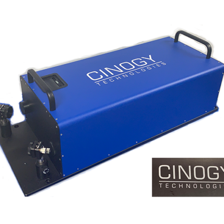
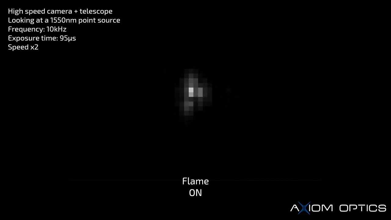
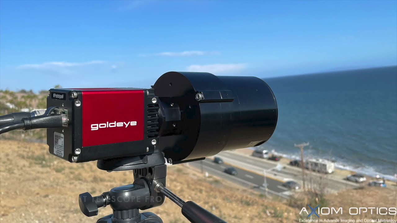
High-speed turbulence imaging of a point source at 1.5 µm using a high-speed SWIR camera and telescope. Acquisition made at 10 kHz with an exposure time of 85 µs and 14-bit pixel depth. In this example, the turbulence consists of induced scintillation with a heat source that changes the refraction index of air. Our high-speed SWIR InGaAs camera solutions are the ideal solution for use in fast adaptive optics and other setups used in FSO (Free-Space Optics) telecommunications.
Video made with: C-RED 3 High-Speed Uncooled InGaAs Camera
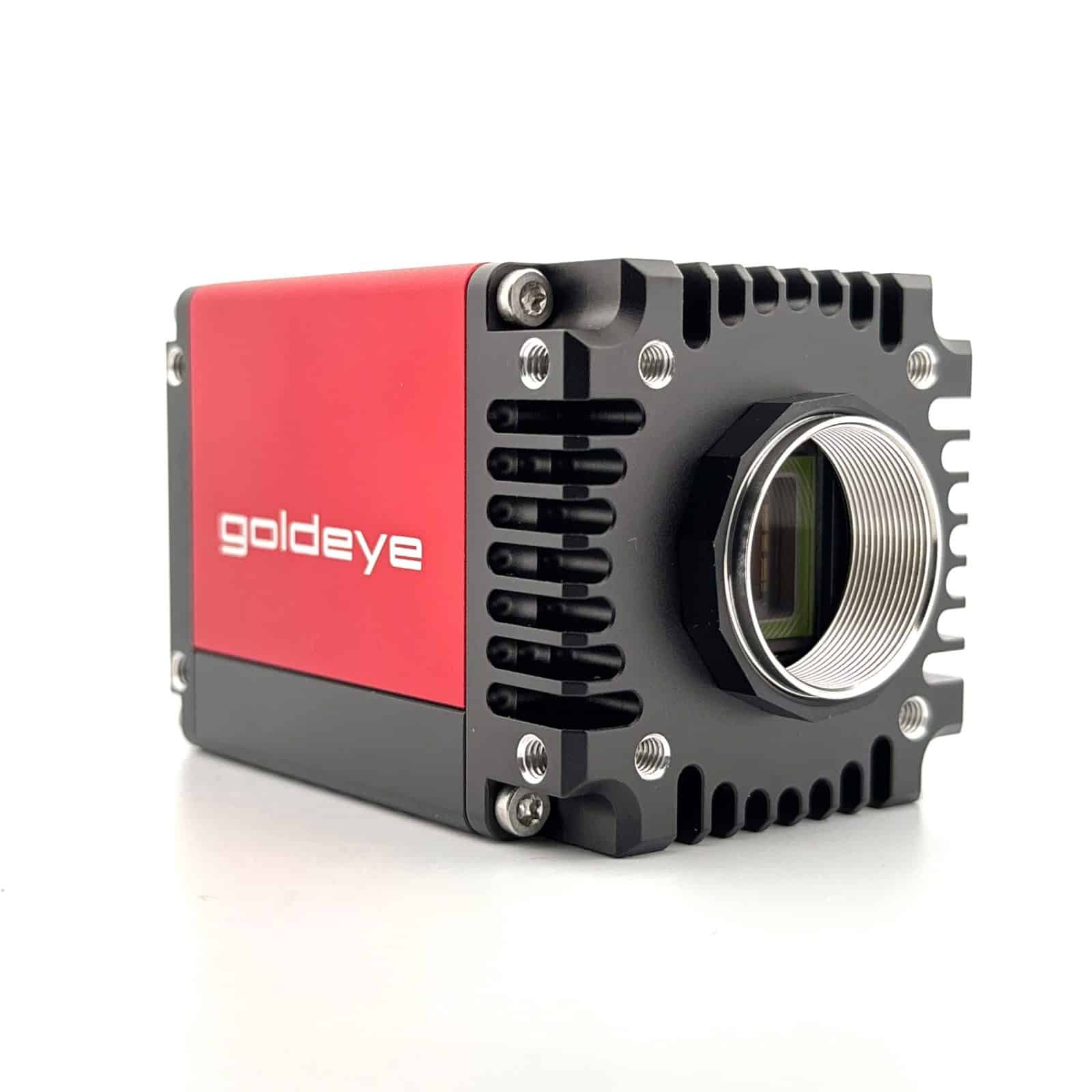
High-resolution imaging is now possible thanks to Sony’s IMX990 InGaAs chip with 1280 x 1024 px resolution and industry’ smallest pixel pitch of 5 µm. SWIR imaging allows high contrast imaging through atmospheric obscurants such as smog or fog.
Video made with: Goldeye VSWIR G-130 TEC1 Camera
High-resolution imaging is now possible thanks to Sony’s IMX990 InGaAs chip with 1280 x 1024 px resolution and industry’ smallest pixel pitch of 5 µm. SWIR imaging allows high contrast imaging through atmospheric obscurants such as smog or fog.
Video made with: Goldeye VSWIR G-130 TEC1 Camera
High-speed imaging of water being poured in the short-wave infrared spectral range. 600 FPS achieved at VGA resolution and 14-bit pixel depth. Higher frame rates can be achieved by windowing down the sensor in both horizontal and vertical directions.
Video made with: C-RED 2 Cooled Scientific Camera
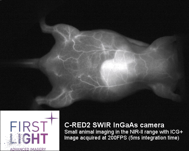
One of the biggest advantages of the SWIR range is that the auto fluorescence is negligible. This low level auto fluorescence increases the contrast and sensitivity compared to conventional imaging in NIR and visible ranges. Some of NIR fluorescence imaging contrast agents such as; ICG (indocyanine green), IRDye800CW and IR-12N3, has a non-negligible long tails passing 1500 nm region (NIR-II/SWIR) [1]. InGaAs (indium gallium arsenide) based SWIR cameras fill the gap for imaging in NIR-II/SWIR wavelength range (900-1700nm) where silicon detectors are no longer sensitive.
Video made with: C-RED2 Cooled InGaAs camera