Introduction to InGaAs
Indium Gallium Arsenide (InGaAs) is a compound semiconductor material that has significantly advanced the capabilities of imaging technology, particularly in the shortwave infrared (SWIR) spectrum. This material is made from a combination of gallium arsenide (GaAs) and indium arsenide (InAs), where the properties can be precisely controlled by adjusting the ratio of indium to gallium. The emergence of InGaAs has opened up new possibilities in various fields such as telecommunications, military, and biomedical imaging.
The Origin of InGaAs
The development of InGaAs began in the latter half of the 20th century as part of the broader exploration into III-V semiconductor materials, which are defined by their position on the periodic table: Group III (including indium and gallium) and Group V (including arsenic). Researchers discovered that by alloying indium arsenide with gallium arsenide, they could effectively bridge the performance gap between the existing semiconductor materials and provide a substrate that was responsive to a broader range of wavelengths, particularly those in the SWIR range.
The unique properties of InGaAs stem from its adjustable bandgap. The bandgap of InGaAs can be tuned from 0.35 eV (indium arsenide) to 1.42 eV (gallium arsenide), allowing devices to be highly sensitive to infrared light without the cooling requirements that materials like mercury cadmium telluride (HgCdTe) demand.
Manufacturing Methods of InGaAs Cameras
The manufacturing of InGaAs cameras, especially those designed for SWIR imaging, involves complex processes tailored to ensure high efficiency and performance across various applications. Here are the primary methods involved:
1. Epitaxial Growth
The foundation of an InGaAs camera is the epitaxial layer of InGaAs semiconductor material grown on a substrate. The most common technique used for this is Metal-Organic Chemical Vapor Deposition (MOCVD). MOCVD allows for precise control over the composition and thickness of the InGaAs layer, which is crucial for the material’s ability to absorb and convert infrared light into electronic signals. Molecular Beam Epitaxy (MBE) is another method, known for its ultra-high vacuum environment that enables the growth of very pure layers.
2. Lithography
Following the growth of the epitaxial layers, lithography is used to pattern the wafers into discrete devices. Photolithography, a process involving light to transfer a geometric pattern from a photomask to a light-sensitive chemical photoresist on the substrate, is commonly used. This step defines the architecture of the photodiodes that will eventually detect and convert the SWIR light into electrical signals.
3. Etching
After patterning, the wafer undergoes etching processes to remove unwanted material. Dry etching techniques, such as reactive ion etching, are often preferred for their ability to provide cleaner and more precise cuts than wet etching. This precision is crucial for maintaining the integrity of the small and densely packed photodiodes in InGaAs cameras.
4. Passivation
Once the photodiodes are formed, the surfaces are passivated to protect them from environmental factors and to reduce noise that could interfere with the detection of SWIR light. This involves depositing a thin layer of material that acts as a barrier against contaminants while also improving the performance of the photodiodes.
5. Hybridization or Cu-Cu bonding.
When manufacturing InGaAs focal plane arrays (FPAs) for shortwave infrared (SWIR) cameras, connecting the InGaAs photodiode array to the readout integrated circuit (ROIC) is a critical step. Two common methods for achieving this connection are hybridization and copper-copper (Cu-Cu) bonding. Each technique has its specific characteristics and advantages, depending on the application’s requirements.
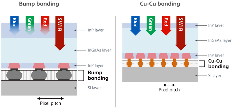
Hybridization
Hybridization typically refers to the use of indium bump bonding to attach the photodiode array to the ROIC. This process involves the following steps:
- Bump Deposition: Indium bumps are deposited on the contact pads of both the photodiode array and the ROIC.
- Alignment and Bonding: The InGaAs array and the ROIC are precisely aligned so that the corresponding bumps match up. They are then pressed together and heated, causing the indium bumps to melt slightly and fuse, creating a mechanical and electrical bond once cooled.
Advantages:
- Thermal Compatibility: Indium has a relatively low melting point (156.6°C), making it suitable for materials sensitive to high temperatures during processing.
- Flexibility in Material Choice: Hybridization allows for the bonding of different types of materials (e.g., InGaAs to silicon), which is beneficial given the different thermal and electronic properties of the photodiode array and the ROIC.
- Proven Reliability: This method has been used extensively and is well-understood, offering reliable performance in a wide range of applications.
- Disadvantages:
- Cost and Complexity: The process of depositing indium bumps and the required alignment equipment can be costly and complex.
- Thermal Expansion Mismatch: The different coefficients of thermal expansion between the InGaAs array and the silicon ROIC can lead to stress and potential failure points over time, especially under varying temperature conditions.
Cu-Cu bonding
Copper-copper bonding is an alternative technique that has been gaining popularity due to its robustness and thermal conductivity. The process includes:
- Surface Preparation: Both the photodiode array and the ROIC are prepared with copper pads at the bonding sites.
- Bonding: The copper surfaces are brought into contact and bonded through a combination of pressure and heat, often under a form of inert atmosphere to prevent oxidation.
Advantages:
- Excellent Thermal and Electrical Conductivity: Copper provides superior conductivity, which can enhance the performance of the FPA by reducing electrical resistance and improving heat dissipation.
- No Intermetallics: Unlike indium or other solder-based methods, Cu-Cu bonding does not involve different metals that could form brittle intermetallic compounds at the interface.
- Scalability and Cost-Effectiveness: Once set up, the Cu-Cu bonding process can be less expensive and easier to scale than indium bump bonding, particularly for large volume production.
- Disadvantages:
- High Bonding Temperature: Cu-Cu bonding typically requires higher temperatures than indium bump bonding, which might not be suitable for all materials or devices sensitive to heat.
- Stringent Surface Preparation: The copper surfaces must be extremely clean and well-prepared to ensure a good bond, which can add complexity to the manufacturing process.
Extending InGaAs to Lower 0r Higher Wavelengths
InGaAs (Indium Gallium Arsenide) is a versatile semiconductor material predominantly used for shortwave infrared (SWIR) detectors. However, the inherent spectral response of standard InGaAs primarily covers wavelengths from approximately 900 nm to 1700 nm. To extend its spectral range, either towards the visible spectrum (shorter wavelengths) or further into the infrared spectrum (longer wavelengths), modifications in its composition and structure are necessary. These modifications result in what is often referred to as “extended InGaAs.”
Extending to Visible Wavelengths (referred to as VSWIR or VIS-SWIR)
To shift the sensitivity of InGaAs detectors towards the visible spectrum, the bandgap of the material needs to be increased. This is achieved by altering the chemical composition of the InGaAs:
- Incorporation of Aluminum (AlInGaAs): Adding aluminum to the InGaAs compound to form aluminum indium gallium arsenide (AlInGaAs) increases the bandgap energy. This adjustment allows the detector to be sensitive to shorter wavelengths, including the visible spectrum. The inclusion of aluminum effectively narrows the bandgap, making the material capable of absorbing photons with higher energies (shorter wavelengths).
- Strain Layer Superlattices: Another method is to use strain layer superlattices, which involve alternating thin layers of materials with slightly different lattice constants. This method can be used to engineer the band structure specifically to enhance performance at desired wavelengths, including extending into the visible range.


Extending to Longer Infrared Wavelengths (referred to as XSWIR or ESWIR)
To extend the detection capability of InGaAs into longer wavelengths, typically towards the mid-infrared range, the bandgap needs to be reduced. This is accomplished by altering the ratio of indium to gallium or by introducing other elements into the lattice:
- Increased Indium Content (In-rich InGaAs): By increasing the proportion of indium in InGaAs, the lattice constant of the material becomes larger, which lowers the bandgap energy. This modification shifts the absorption edge of the detector to longer wavelengths, potentially up to about 2.6 micrometers.
- Doping with Other Elements: Doping InGaAs with elements like nitrogen can also adjust the band structure to extend the absorption into the longer wavelengths. Nitrogen incorporation introduces intermediate energy states within the bandgap, effectively narrowing it.
- Engineering of Quantum Wells: Using quantum well structures within the InGaAs matrix can allow for the engineering of electronic states to achieve sensitivity at specific longer wavelengths. These wells confine carriers in potential wells that have discrete energy levels, which can be tuned by adjusting the well width and barrier height.
Applications and Implications
The ability to modify InGaAs to extend its spectral range enhances its versatility for various applications:
- Visible Extensions: Devices that can detect both visible and near-infrared light are crucial for applications such as color night vision and multispectral imaging in agriculture and environmental monitoring.
- Infrared Extensions: Extending the wavelength range into the mid-infrared can be vital for applications in non-invasive medical diagnostics, chemical spectroscopy, and long-range thermal imaging in defense and security.
These modifications not only broaden the applicability of InGaAs-based detectors but also push the boundaries of what can be achieved with semiconductor technology in imaging and sensing across diverse fields.
